
Assignment 4: Basic pipelining
Due: 5:00pm, Thu 15 Feb. Value: 30 pts. Submit to Moodle.
In this assignment, we'll explore what it takes to convert an unpipelined processor design to use a four-stage pipeline instead. We'll deal with data hazards through forwarding, and we'll deal with control hazards through stalling. I think you'll find that if you start with a well-designed framework, pipelining is surprisingly simple.
For this assignment, we'll be using Logisim [Logisim home]. The project file mips-fwrd.circ [Download] contains an unpipelined implementation for a tweaked MIPS instruction set. Modifications to MIPS include the following:
The only instructions supported are the basic ALU operations (
add,sub,addi,addu,subu,addiu,and,or,nor,xor,andi,or,xori,lui,sll,srl,sra,sllv,srlv,srav,slt,sltu,slti,sltiu) and the two branch instructions (beq,bne). Omitted instruction categories include: load/store, unconditional jumps (or calls), multiply/divide.(Note that, since there are no load/store instructions, our pipeline won't need a MEM stage. Thus, our pipeline will have four stages: instruction fetch (IF), instruction decode (ID), execute (EX), and write-back (WB).)
Branch instructions do not observe a branch delay slot in the distributed circuit. However, after Part A, your solution circuit will end up implementing delay slots, almost by accident. They will be removed again in Part C.
No instructions lead to exceptions. For example, no overflow exception can result from
add, so theaddinstruction works identically toaddu.When the circuit reaches an unrecognized instruction (including unsupported instructions such as
lw), it simply treats it as a no-op (rather than initiating an exception).At center top, you can see that there is an area labeled “
$v0”. This is simply wired directly to the corresponding register, which allows a program executing to have a current output (displayed in hexadecimal).
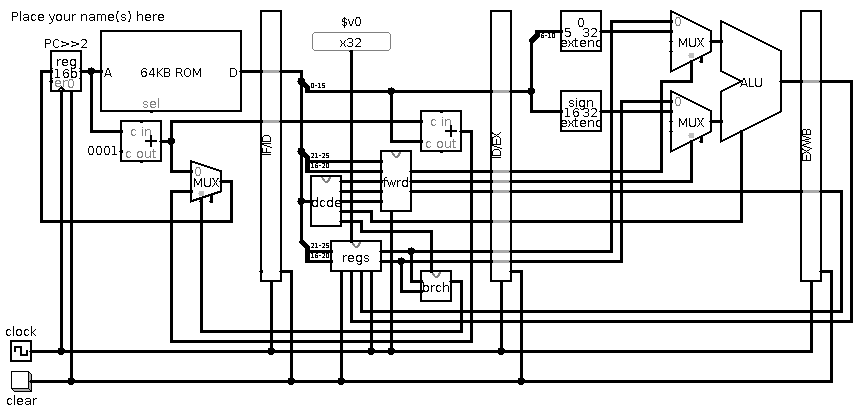
The circuit has three tall rectangles that appear to be pipeline registers, suggesting a four-stage pipeline. In the circuit as distributed, though, these “pipeline registers” simply pass inputs from one “stage” to the next without any delay. Thus, the distributed circuit reads and completes a full instruction with each clock cycle; there is no pipeline. Your job in this assignment is to modify the circuit to implement pipelining, as described below in Part A, Part B, and Part C. Submit your completed solution as outlined below.
Do not modify any subcircuits except those outlined below.
Part A: Pipeline registers
We begin by modifying the “pipeline registers” to actually work as pipeline registers.
In the “main” circuit, edit the “Place your name(s) here” label to instead include your name(s).
In the IF/ID, ID/EX, and EX/WB circuits, insert a register between each input/output pair, controlled by the clock input. Important: Each register should be configured to be triggered by a “falling edge” of the clock. This is because the rest of the circuit is built imagining that a clock cycle begins when the clock goes from 1 down to 0.
In adding each register, you'll want to connect the circuit's “clock” input to the triangle input at the register's bottom edge. You'll also want to connect the circuit's “clear” input to the 0 input at the triangle's bottom edge.
At this point, you can test your circuit, as outlined under “Testing” below. Two caveats:
Each branch instruction will observe a branch delay slot. This will happen automatically when you add registers into the IF/ID stage. It is expected behavior, but of course it affects how you write your test code.
Your circuit does not yet deal with data hazards. So if an instruction reads a register that would be modified by the immediately preceding instruction, it will actually see the register value before completing that preceding instruction. We'll repair this in Part B, but to test Part A you can insert a
nopinstruction between any such instruction pair.
Part B: Data hazards & forwarding
Now we'll modify the circuit to deal with data hazards.
In the “main” circuit, add wires that send the result from the WB stage as an additional option for each of the two multiplexers in the EX stage. This will give a way for an instruction entering EX to receive the result from the preceding instruction (when that instruction's result is sitting in the WB stage) — but we need to configure the multiplexer to receive it, which we do next.
Now modify the “forward” circuit; as distributed, it simply passes its inputs through. While this circuit needn't be tremendously complex after completion, it does take some careful thinking. The “forward” circuit takes six inputs.
source register 0: The ID number for the first register that the instruction reads (if it needs it). For example, for the instruction “
add $2, $4, $5”, this value would be 4.source register 1: The ID number for the second register that the instruction reads (if it needs it). For the instruction “
add $2, $4, $5”, this value would be 5.operand 0 select: 0 if the register value is used for the first operand, 1 if an immediate should be used (such as for
sllorsra).operand 1 select: 0 if the register value is used for the second operand, 1 if an immediate should be used (such as for
addiorlui).destination register: The ID number for the register where the current instruction's result should be placed. Note that this will be 0 if the instruction should have no effect (such as a branch instruction or an invalid instruction).
clock: The current clock for the circuit. You'll want this because you'll want to insert a register to remember the destination register from the previous clock cycle.
The circuit has three outputs.
operand 0 select: The select input for the EX stage's upper multiplexer. This two-bit value should be 00 to use the first register value read in the ID stage; it should be 01 to use the shift-distance value found in the instruction (such as with
sllorsra); and it should be something else if the ALU's first operand should be the result of the instruction immediately preceding.operand 1 select: The select input for the EX stage's lower multiplexer. This two-bit value should be 00 to use the second register value read in the ID stage; it should be 01 to use the immediate value found in the instruction (such as with
addiorlui); and it should be something else if the ALU's second operand should be the result of the instruction immediately preceding.destination register: The ID number for the register where the current instruction's result should be placed. This will simply match the corresponding input.
You'll want to avoid attempts to forward register 0. Consider the following simple program.
addi $0, $0, 1
add $v0, $0, $0
Register 0 is constant-0 under MIPS, so the first instruction should do nothing. However, if the circuit erroneously forwards the
addiinstruction's result (which will be 1) as theaddinstruction is in the EX stage, it will end up placing 2 into$v0.(Admittedly, nobody should have a reason to write this example program, but nonetheless the circuit needs to handle it according to MIPS specifications correctly. Actually, there is a more realistic scenario: The decode unit handles branch instructions (and invalid instructions) by using 0 for the destination register, though the ALU still does work. If a branch is followed with an instruction using register 0, and if you forward the branch's “result” to it, then that instruction could receive a value that was never intended to be used.)
Test your circuit as outlined under “Testing” below.
Part C: Control hazards & stalling
Finally, we will modify the circuit to handle control hazards. The effect of this will be to reinstate the no-delay-slot behavior as originally specified.
In “main” circuit's IF stage, note that there is a wire controlling the multiplexer; a value of 1 indicates that the PC is to change to the branch destination. Connect this wire also to the IF/ID pipeline register's “enable” input (found at lower left, across from the lower right input connected to the “clear” button).
Modify the IF/ID circuit so that when the “enable” input is 1 (indicating a branch is being taken), the instruction register's D input will be 0. In this way, when a branch is being taken, the instruction inserted into the IF/ID stage (which would be the one from the delay slot) changes to a no-op.
Test your circuit as outlined under “Testing” below.
Submit your completed solution as outlined below.
Testing
Begin by using MARS to compose the program you wish to use to test your circuit. I suggest using the updated version (4.2hx2) already installed in the lab. [Download]
Of course, the program you write should use only the instructions that the circuit supports, as listed above. I suggest placing any result value into
$v0so it will be easily visible.I suggest testing the program within MARS before attempting to see how it works in your circuit. If you're testing Part A or Part B, your circuit will have a delay slot for each branch, so within MARS you'll want to enable “Delayed branching” from the Settings menu so that MARS simulates delay slots as well.
After ensuring that the program works as you expect within MARS, select “Dump Memory…” from the File menu, and save the resulting data into a file. (In an older MARS version, such as the one from Assignment 2, insert an extra step here: Select the Hexadecimal Text format (selected by default in 4.2hx2); after saving, edit the resulting file in a text editor to add the line “
v2.0 raw” at the file's top, which Logisim will require.)Enter Logisim, right-click (or control-click) the ROM in the “main” circuit's upper left corner, select “Load Image…”, and select the dump file you created.
Ensure the clock is at 0; if it is at 1, select the Poke Tool (the hand icon) and click the clock in the bottom left corner to bring it back to 0.
With the Poke Tool (the hand icon) selected, click the clear button in the circuit's bottom left corner to reset the PC and all registers to 0.
To execute the program, you can repeatedly click the clock using the Poke Tool to step one half-cycle at a time, or you can select “Ticks Enabled” from the Simulate menu to start the clock running automatically through the program. (You can slow its speed through the “Tick Frequency” submenu.)
To view current register values, right-click the “regs” circuit and select “View registers”. You can double-click “main” to go back to the overall circuit.
Submitting your solution
Your completed solution should include two files.
- the Logisim project file after completing Part C.
- the MARS assembly code file representing the most sophisticated test you used for verifying your project's correctness. This program need not be neat or extensive, but it should reflect reasonably thorough testing of your circuit's correctness.